Traceable Laser Marking for Electronics | ESD-Safe
Laser Marking for Semiconductors and Electronics
Objective in Context
Electronics manufacturers lose up to 3% in annual revenue due to untraceable field failures and counterfeit components. Non-conductive, permanent laser marking (keyword: electronic laser marking) enables full traceability from wafer to SMT line and significantly reduces rework and warranty costs.
Scope & Level
End-to-end traceability across the entire supply chain (Sea Level)
Stakeholders
- Primary: SMT Process Engineer
- Also involved: Quality Assurance, Suppliers, Customer RMA Team, MES System
Trigger
A new product SKU enters full-scale production and must be integrated into automated SMT manufacturing.
Pre- / Post-Conditions
- Components are unmarked
- MES awaits serial number input
- Each unit carries a unique, ESD-safe laser ID
- Fully traceable in the MES
Main Scenario
Process Engineer defines marking parameters via laser station UI
System validates material and ESD sensitivity
Component tray enters shielded laser cell
Vision system identifies microchip orientation (±5 µm accuracy)
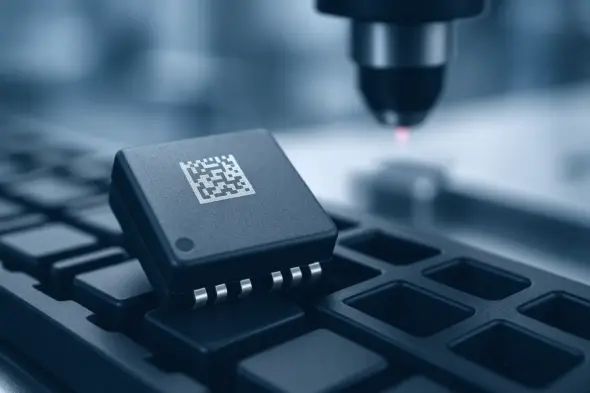
Fiber laser applies non-conductive Data Matrix code (30 ms)
Inline camera verifies ≥99.8% readability
Serial number is reported back to MES / ERP
Conveyor passes component to SMT placement line
Downstream AOI reads code and confirms linkage
In case of field failure, the RMA portal scans the code and traces root cause back to lot and EBOM

Sequence Diagram
Alternative / Exception Paths
Orientation error
Particle contamination
No SN reservation
KPIs / Key Metrics
| KPI | Target | Benchmark (est.) |
|---|---|---|
| First-pass mark yield | ≥ 99.5% | 98% industry average |
| Traceability coverage | 100% of units | 92% |
| RMA cost reduction | –25% within 12 months | – |
| Readability after 500 reflow cycles | >99% | – |
ROI Calculation
| Year | CAPEX [€] | OPEX [€] (Maintenance) | *Annual Savings [€] ** | Net Cashflow [€] | Cumulative [€] |
|---|---|---|---|---|---|
| 0 | –145,000 | – | – | –145,000 | –145,000 |
| 1 | – | 8,000 | 105,000 | +97,000 | –48,000 |
| 2 | – | 8,000 | 105,000 | +97,000 | +49,000 |
| 3 | – | 8,000 | 105,000 | +97,000 | +146,000 |
Key Assumptions
*Annual Savings:
- - €75,000: 25% reduction in RMA-related costs
- - €20,000: Less scrap due to failed markings
- - €10,000: Lower manual rework
Payback Period: ~1.5 years | 3-Year ROI: ~101%
(*All figures in EUR, based on 120k€ laser station + 20k€ integration + 5k€ training, no discounting for simplicity.)
Interpretation
Fast Payback in Electronics Manufacturing
With a payback period of ~1.5 years, the investment is recovered well before the end of year two. In electronics manufacturing, a return within 3 years is considered a "fast payback", giving this solution a clear edge over other traceability approaches.
Cashflow Driver: RMA Reduction
75% of the annual savings come from reduced warranty and RMA effort (–25% p.a.). The main leverage: Every claimed assembly can be rapidly traced back to the responsible process settings and lot, thanks to the unique serial number. The larger the installed base, the stronger this scaling effect.
Line-Level Quality Boost
Another €20,000 per year is saved by reducing SMT scrap. Inline verification (≥99.8% readability) prevents costly late-stage rework. Avoiding mis-mark cycles saves ~2 minutes of handling time per unit—at 50k UPH, that adds up quickly.
Long-Term Profitability
After 3 years, the cumulative net cashflow is €146,000, resulting in an ROI of ~101%. Even if savings are only 70% of forecast (e.g. due to lower RMA leverage), ROI remains above 40%—still a solid return.
Risk & Sensitivity Analysis
Factor Positive Case Negative Case Comment RMA Rate –30% –10% Most sensitive lever; strongly correlated with product complexity Marker Availability 98% 92% Redundant laser recommended above 80k UPH OPEX increase (maint.) +2% p.a. +8% p.a. Service contract stabilizes costs—low risk Intangible Benefits (qualitative)
- Brand Protection & Anti-Counterfeiting strengthen perceived value
- Proactive compliance with regulations like the US CHIPS Act and EU Digital Product Passport
- Faster root-cause analysis improves customer satisfaction and lowers cost of poor quality